20
LTC1968
1968f
V
OUT
= ((5mV AC)
2
+ (0.4mV DC)
2
) " 1.001 + 0.2mV
= 5.221mV
= 5mV + 4.42%
As can be seen, the gain term dominates with large inputs,
while the offset terms become significant with smaller
inputs. In fact, 5mV is the minimum RMS level needed to
keep the LTC1968 calculation core functioning normally,
so this represents the worst-case of usable input levels.
Using the worst-case values of the LTC1968 static errors,
the total conversion error is:
V
OUT
= ((500mV AC)
2
+ (1.5mV DC)
2
) " 1.003 + 0.75mV
= 502.25mV
= 500mV + 0.45%
V
OUT
= ((50mV AC)
2
+ (1.5mV DC)
2
) " 1.003 + 0.75mV
= 50.923mV
= 50mV + 1.85%
V
OUT
= ((5mV AC)
2
+ (1.5mV DC)
2
) " 1.003 + 0.75mV
= 5.986mV
= 5mV + 19.7%
These static error terms are in addition to dynamic error
terms that depend on the input signal. See the Design
Cookbook for a discussion of the DC conversion error with
low frequency AC inputs. The LTC1968 bandwidth limita-
tions cause additional errors with high frequency inputs.
Another dynamic error is due to crest factor. The LTC1968
performance versus crest factor is shown in the Typical
Performance Characteristics.
Output Errors Versus Frequency
As mentioned in the design cookbook, the LTC1968 per-
forms very well with low frequency and very low frequency
inputs, provided a large enough averaging capacitor is used.
However, the LTC1968 will have additional dynamic errors
as the input frequency is increased. The LTC1968 is de-
signed for high accuracy RMS-to-DC conversion of sig-
nals up to 100kHz. However, the switched capacitor cir-
cuitry samples the inputs at a modest 2MHz nominal. The
response versus frequency is depicted in the Typical Per-
formance Characteristics titled Input Signal Bandwidth.
APPLICATIO S I FOR ATIO
U
U
U
Although there is a pattern to the response versus fre-
quency that repeats every sample frequency, the errors
are not overwhelming. This is because LTC1968 RMS
calculation is inherently wideband, operating properly with
minimal oversampling, or even undersampling, using sev-
eral proprietary techniques to exploit the fact that the RMS
value of an aliased signal is the same as the RMS value of
the original signal. However, a fundamental feature of the
?modulator is that sample estimation noise is shaped
such that minimal noise occurs with input frequencies
much less than the sampling frequency, but such noise
peaks when input frequency reaches half the sampling
frequency. Fortunately the LTC1968 output averaging fil-
ter greatly reduces this error, but the RMS-to-DC topology
frequency shifts the noise to low (baseband) frequencies.
See Output Noise vs Input Frequency in the Typical Perfor-
mance Characteristics.
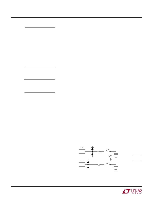
Input Impedance
The LTC1968 true RMS-to-DC converter utilizes a 0.8pF
capacitor to sample the input at a nominal 2MHz sample
frequency. This accounts for the 1.2M& input impedance.
See Figure 20 for the equivalent analog input circuit. Note
however, that the 1.2M& input impedance does not di-
rectly affect the input sampling accuracy. For instance, if
a 15.5k source resistance is used to drive the LTC1968, the
sampling action of the input stage will drag down the
voltage seen at the input pins with small spikes at every
sample clock edge as the sample capacitor is connected to
be charged. The time constant of this combination is
small, 0.8pF " 15.5k& = 12.5ns, and during the 125ns
period devoted to sampling, ten time constants elapse.
Figure 20. LTC1968 Equivalent Analog Input Circuit
IN1
V
DD
V
DD
V
SS
V
SS
R
SW
(TYP)
2k
C
EQ
0.8pF
(TYP)
C
EQ
0.8pF
(TYP)
I
IN1
IN2
I
IN2
1968 F20
R
SW
(TYP)
2k
IIN
V V
R
IIN
V V
R
R
M
AVG
IN IN
EQ
AVG
IN IN
EQ
EQ
1
2
1.2
1 2
2 1
( )
=
( )
=
=
&
发布紧急采购,3分钟左右您将得到回复。
相关PDF资料
LTC3100EUD#TRPBF
IC REG BUCK/BOOST/LINEAR 16-QFN
LTC3104IMSE#TRPBF
IC REG DL BCK/LINEAR SYNC 16MSOP
LTC3445EUF#TRPBF
IC REG TRPL BUCK/LINEAR 24-QFN
LTC3446IDE#PBF
IC REG TRPL BCK/LINEAR 14-DFN
LTC3537EUD#TRPBF
IC REG DL BST/LINEAR SYNC 16-QFN
LTC3541EDD#TRPBF
IC REG DL BCK/LINEAR SYNC 10-DFN
LTC3670EDDB#TRPBF
IC REG TRPL BCK/LINEAR 12DFN
LTC3672BEDC-1#TRPBF
IC REG TRPL BCK/LINEAR 8-DFN
相关代理商/技术参数
LTC1980EGN
功能描述:IC PWM BATT CHARGER/CONV 24-SSOP RoHS:否 类别:集成电路 (IC) >> PMIC - 电池管理 系列:- 产品培训模块:Lead (SnPb) Finish for COTS
Obsolescence Mitigation Program 标准包装:2,500 系列:- 功能:电池监控器 电池化学:碱性,锂离子,镍镉,镍金属氢化物 电源电压:1 V ~ 5.5 V 工作温度:-40°C ~ 85°C 安装类型:表面贴装 封装/外壳:SOT-23-6 供应商设备封装:SOT-6 包装:带卷 (TR)
LTC1980EGN#PBF
功能描述:IC PWM BATT CHARGER/CONV 24-SSOP RoHS:是 类别:集成电路 (IC) >> PMIC - 电池管理 系列:- 产品培训模块:Lead (SnPb) Finish for COTS
Obsolescence Mitigation Program 标准包装:2,500 系列:- 功能:电池监控器 电池化学:碱性,锂离子,镍镉,镍金属氢化物 电源电压:1 V ~ 5.5 V 工作温度:-40°C ~ 85°C 安装类型:表面贴装 封装/外壳:SOT-23-6 供应商设备封装:SOT-6 包装:带卷 (TR)
LTC1980EGN#TR
功能描述:IC PWM BATT CHARGER/CONV 24-SSOP RoHS:否 类别:集成电路 (IC) >> PMIC - 电池管理 系列:- 产品培训模块:Lead (SnPb) Finish for COTS
Obsolescence Mitigation Program 标准包装:2,500 系列:- 功能:电池监控器 电池化学:碱性,锂离子,镍镉,镍金属氢化物 电源电压:1 V ~ 5.5 V 工作温度:-40°C ~ 85°C 安装类型:表面贴装 封装/外壳:SOT-23-6 供应商设备封装:SOT-6 包装:带卷 (TR)
LTC1980EGN#TRPBF
功能描述:IC PWM BATT CHARGER/CONV 24-SSOP RoHS:是 类别:集成电路 (IC) >> PMIC - 电池管理 系列:- 产品培训模块:Lead (SnPb) Finish for COTS
Obsolescence Mitigation Program 标准包装:2,500 系列:- 功能:电池监控器 电池化学:碱性,锂离子,镍镉,镍金属氢化物 电源电压:1 V ~ 5.5 V 工作温度:-40°C ~ 85°C 安装类型:表面贴装 封装/外壳:SOT-23-6 供应商设备封装:SOT-6 包装:带卷 (TR)
LTC1981ES5
制造商:Linear Technology 功能描述:MOSFET DRVR 1-OUT Hi Side 5-Pin TSOT-23
LTC1981ES5#PBF
制造商:Linear Technology 功能描述:MOSFET DRVR 1-OUT Hi Side 5-Pin TSOT-23 制造商:Linear Technology 功能描述:DP-Power Controller, CUT TAPE Single Micropower Hi Side Sw Controller 制造商:Linear Technology 功能描述:DRIVER, MOSFET, HIGH/LOW SIDE, SOT-23, Device Type:MOSFET, Module Configuration:High Side, Low Side, Supply Voltage Min:1.8V, Supply Voltage Max:5.5V, Driver Case Style:SOT-23, No. of Pins:5, Operating Temperature Min:-40C , RoHS Compliant: Yes
LTC1981ES5#TR
功能描述:IC HI-SIDE SW CTRL SNGL TSOT23-5 RoHS:否 类别:集成电路 (IC) >> PMIC - MOSFET,电桥驱动器 - 外部开关 系列:- 标准包装:50 系列:- 配置:低端 输入类型:非反相 延迟时间:40ns 电流 - 峰:9A 配置数:1 输出数:1 高端电压 - 最大(自引导启动):- 电源电压:4.5 V ~ 35 V 工作温度:-40°C ~ 125°C 安装类型:表面贴装 封装/外壳:TO-263-6,D²Pak(5 引线+接片),TO-263BA 供应商设备封装:TO-263 包装:管件
LTC1981ES5#TRM
功能描述:IC HI-SIDE SW CTRL SNGL TSOT23-5 RoHS:否 类别:集成电路 (IC) >> PMIC - MOSFET,电桥驱动器 - 外部开关 系列:- 标准包装:50 系列:- 配置:高端 输入类型:非反相 延迟时间:200ns 电流 - 峰:250mA 配置数:1 输出数:1 高端电压 - 最大(自引导启动):600V 电源电压:12 V ~ 20 V 工作温度:-40°C ~ 125°C 安装类型:通孔 封装/外壳:8-DIP(0.300",7.62mm) 供应商设备封装:8-DIP 包装:管件 其它名称:*IR2127